Build Blog 4: Electrical Progress
- Abhinav Agrahari

- Feb 17, 2023
- 3 min read
Hi everyone! This week's blog post is focused on our electrical progress, and the related integration work.
Electrical
Overview
Last term we designed the schematic and approximate PCB layout. In last week's blog post, we mentioned that we received our PCB from a manufacturer! I'd like to first take a step back and walk through the manufacturing process, and then discuss further progress.
Our custom PCB enables control and interfacing a Raspberry with several liquid level sensors, 12V peristaltic pumps, a few temperature sensors, and remote controllable outlets.
Breadboard Tests
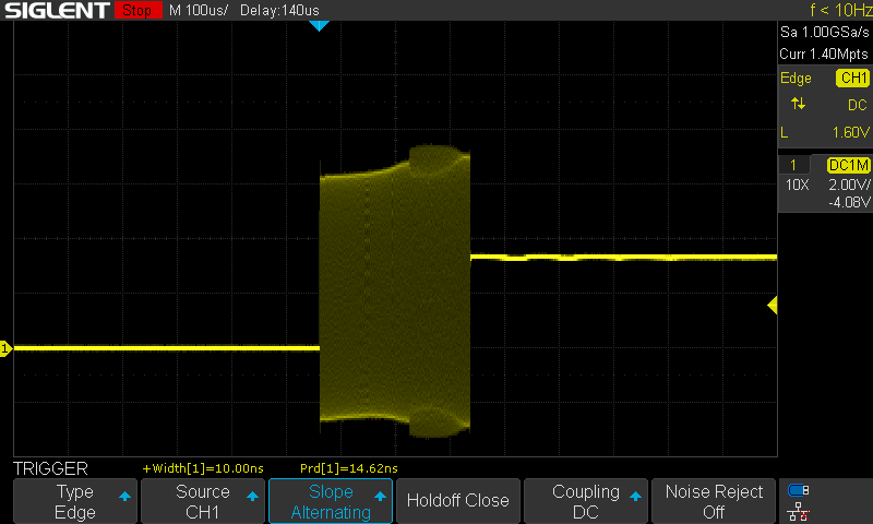
Before beginning the PCB layout, the first step was to verify our schematics via a Breadboard Test. These tests provided great insight and verification at a unit-design level. Below is one such test - this design ensures our PCB operates only at the 'low-power' level.

Through testing, it was found that some of the level sensor input signals experience ringing, due to their long wires (not shown). Important things to account for when designing the PCB!

After updating the schematic based on these breadboard tests, the next step was to layout the PCB.
PCB Layout
We decided to use the open-source EDA tool, KiCad 6.0, for this. After creating footprints from scratch, verifying them with physical dimensions, and importing 3D models into KiCad, we roughly placed the components in a first-iteration of the layout. Quite clear that a 10cmx10cm PCB would be too small!

After increasing the board size, and further refining the layout, I came up with the layout shown below. Much cleaner!

The next step in PCB layout is usually to route all signals, before adding silkscreen text. However, given this is a fairly modular, simple, and well-layed out board, I decided to add the silkscreen first:

Then, I routed all signals between each components. If you're familiar with KiCad, you'll notice that I made the top layer a ground pour, and routed as many signals as possible on the bottom of the board. This lets the user-facing side of the PCB to have a sleek look and solid silkscreen text.
Here's some final 3D models of the PCB with the breakout boards we're using:
Manufacturing
A couple of weeks ago, we had sent out our PCB design to get manufactured, and as mentioned, it came in last week! Here is the bare PCB we received:
Assembly Update
This week, we worked on soldering components to the PCB and performing individual component and unit testing. Here's the PCB after soldering on all our components:

And After attaching all breakout boards and IC's being used:

Here's some additional pictures of our completed PCB. Swipe right!
Testing
After assembling the PCB, we also performed individual component and unit testing. Here's our PCB connected to a Raspberry Pi and 12V adapter, and lighting up some LEDs. The classical PCB bring-up step of BinkyLED was a success!

Mechanical Integration
Besides PCB assembly and testing, we also ironed out some electrical and mechanical integration items.
Testing Sensor Interference
The Liquid Level Sensor selected, through testing, was found to give false readings when near a metal surface.
Since the plant trays will be made from food-safe stainless-steel, this would be an issue! To solve, this, the plant tray design was iterated upon and a small plastic window cutout will be placed for the level sensors.

Electronics Enclosure
The team has also finalized the electronics enclosure design, shown in the CAD model below. All high-power electrical equipment resides in the lower-half of the box, while the top half contains our custom PCB and circuitry. We are currently working manufacturing this, along with other mechanical aspects

Stay tuned for more updates next week!


Comments